We've recently had to send some of our boards back to PCBA after uncovering some faults in them that we didn't notice initially. The issues are easily fixable, but generally: running up against board flaws at the last second is both costly and time-consuming. To help debug issues like these faster, we gained access to an X-ray machine, which can help identify the root cause of potential board flaws.
Ordinarily, a PCBA would do an X-ray inspection as part of the production process; however, not every PCBA has this capability, and it's not always done for every board. Especially during prototyping: being able to narrow down an issue quickly is important. Below we show off some X-ray shots of our boards, and identify a few (potential) board faults, as a demonstration of their usefulness.
1 X-Ray Board Shots
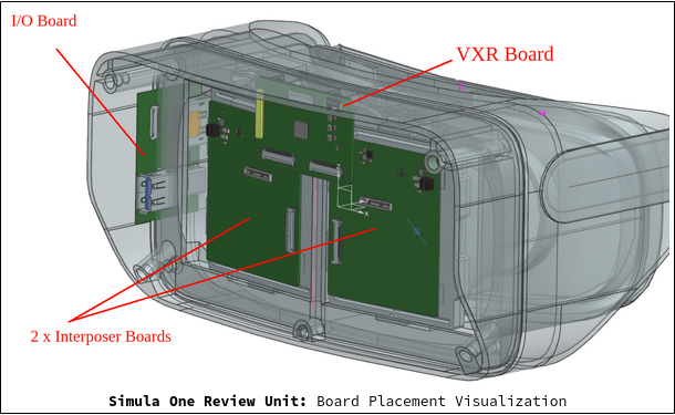
Recall our main board placement schema:
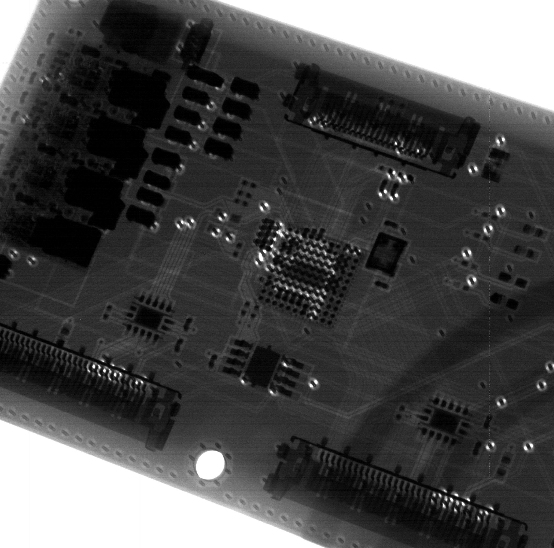
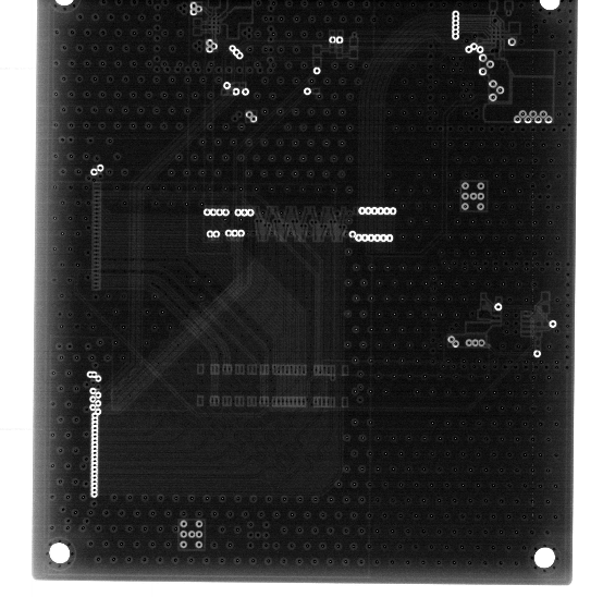
1.1 VXR Board X-Rays
Recall that our VXR PCB is the board which splits a DisplayPort link from our compute pack into two MIPI-DSI links (which are then fed into our VR displays). Here's what they look like assembled:

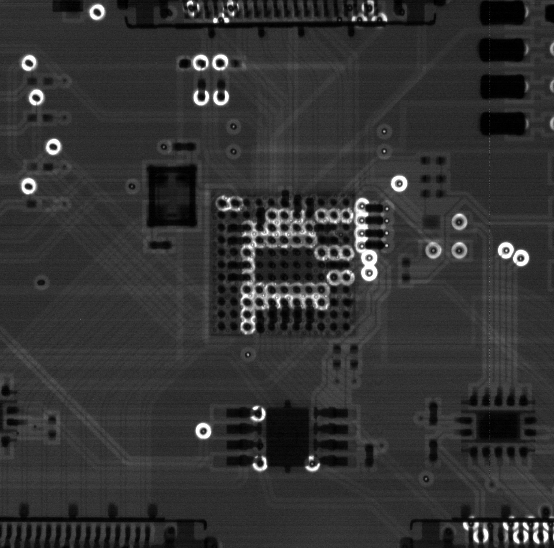
And here are some X-Ray shots, starting first with some flat ones (the boards in these images are those we had at hand, so there might be some components missing):
We can also illustrate a 3D effect by propping the sample up at an angle (in order to get a reconstructable image it'd need to be rotated more precisely):
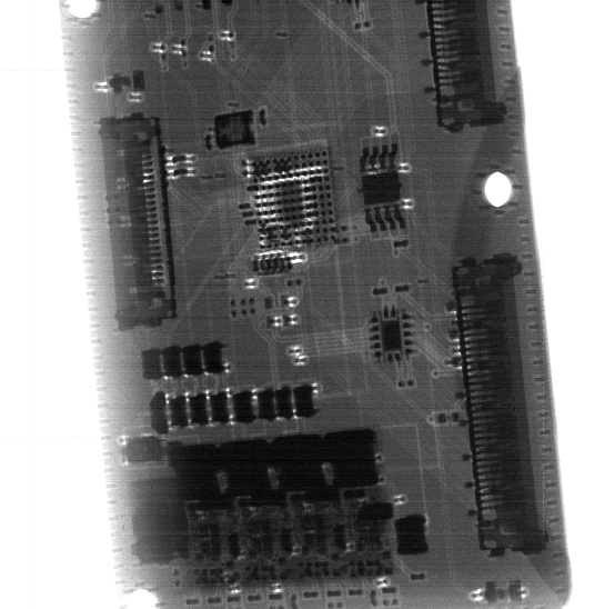

In general, more advanced imaging has more penetrating power and can give clearer images. It can even show a full 3D image if you do a CT scan. While increasing the X-ray voltage isn't feasible with this setup, it's possible to reconstruct a fuller 3D image by rotating the sample and shooting multiple pictures.
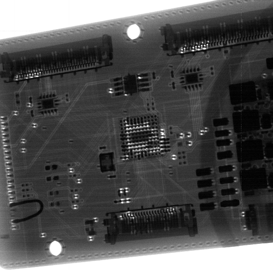
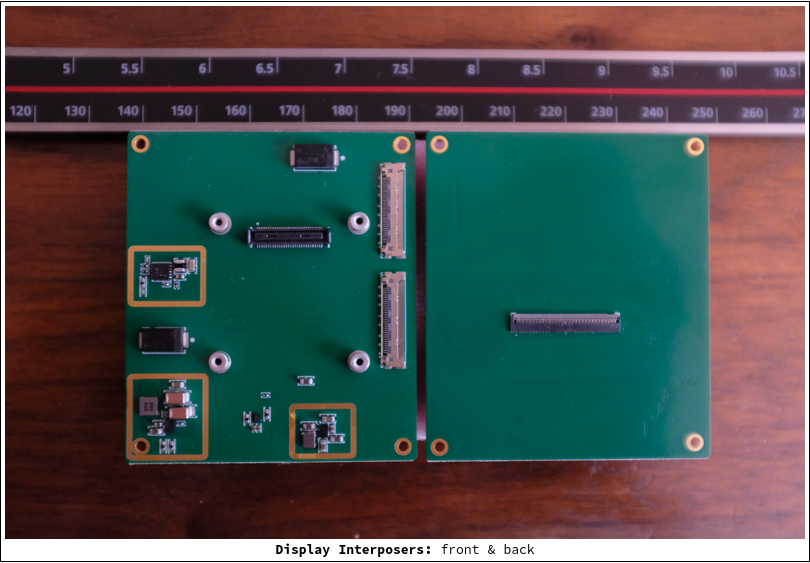
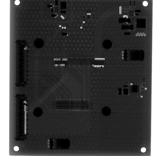
1.2 Display Interposer X-Rays
Recall that these boards connect our VR displays to the VXR board (and cameras to an FPGA board). Here's what they look like assembled:
And here are some X-Ray shots:
1.3 Connector Board X-Rays (Omitted)
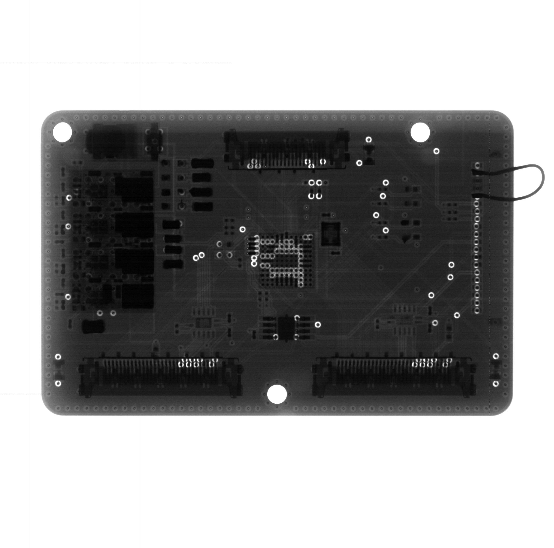
Our "Connector Board" refers to an I/O PCB which connects our compute unit to the VXR and Intel RealSense (used for positional tracking in our review units). Here's a front and back shot:

We omitted X-raying our connector boards on this go around for two reasons: (i) it's relatively easy to just manually test the functionality of these boards without an X-ray; (ii) we didn't have any free boards lying around during the time of X-raying :)
2 Discovering Potential Imperfections
2.1 PCB Bridges
The main flaw we've been on the look out for when scanning our boards are PCB bridges, which are erroneous connections between two copper pads:
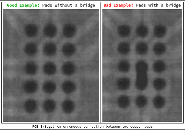
We believe PCB bridges were the problem with some of the boards we recently returned to PCBA, though we can't prove it with X-rays scans since we already returned the boards for repair.
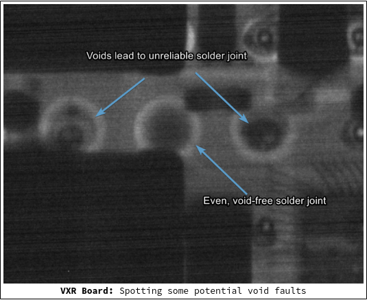
2.2 PCB Voids
Another issue we've been on the lookout for are PCB voids, which are depressions on PCBs which can cause electrical shorts or poor signal integrity. They are typically created when a board is etched (during the manufacturing process), or by poor soldering or plating. Here's an example of what they look like:
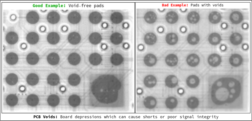
After scanning a couple of our VXR boards (pictured above), we actually found some potential PCB voids. First, here are two boards we scanned, shown one after the other (flipping between them like this makes makes it easier to spot their differences):

If we zoom in a bit, we can spot some potential void faults: