We have recently been working on an FPGA Board to help process camera data for Simula's AR Mode. We've recently made some block diagrams which show the signal flow from the Camera Boards to the FPGA to the Host. Below, we show these diagrams, and then discuss the image processing pipeline inside the FPGA.
1 FPGA Block Diagrams
1.1 Camera Boards -> FPGA
We have two diagrams describing signal flow from the Camera Boards to the FPGA.
1.1.1 Image Data Flow (SLVS-EC)
The first and most important diagram explains how image data flows from the Camera Boards to the FPGA via SLVS-EC. (Note that boxes in blue denote non-FPGA boards, boxes in white denote interfaces, and boxes in yellow mark FPGA abstractions):
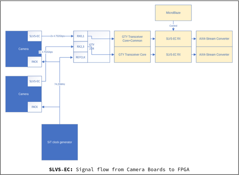
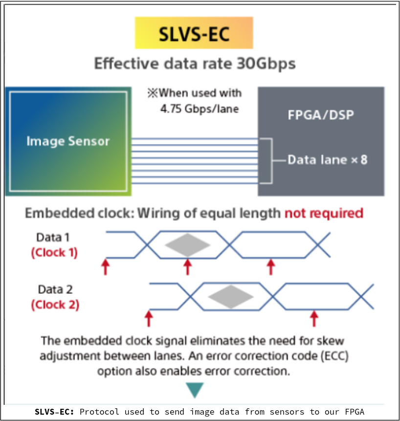
SLVS-EC is the protocol we are using to route images from our Camera Boards to our new FPGA board. It stands for "Scalable Low-Voltage Signaling with Embedded Clock", and is developed by Sony. It features an embedded clock signal, supports up to 8 lanes (including multiple streams or sensors at once).
Some other terms used in the diagram:
- INCK: Stands for "Input Clock"
- GTY. A transceiver block used in Xilinx FPGAs for high-speed communication interfaces
RX*: Stands for receiver channels- REFCLK: Stands for "Reference Clock"
- MicroBlaze: A soft microprocessor IP core provided by Xilinx
- AXI4-Stream: A protocol designed for transporting arbitrary unidirectional data
1.1.2 Camera Control
The second diagram shows the Camera Control signals going between Camera Boards and the FPGA (see the next section for some examples of these signals). SPI stands for "Serial Peripheral Interface", which is another communication protocol used for exchanging data between digital devices:
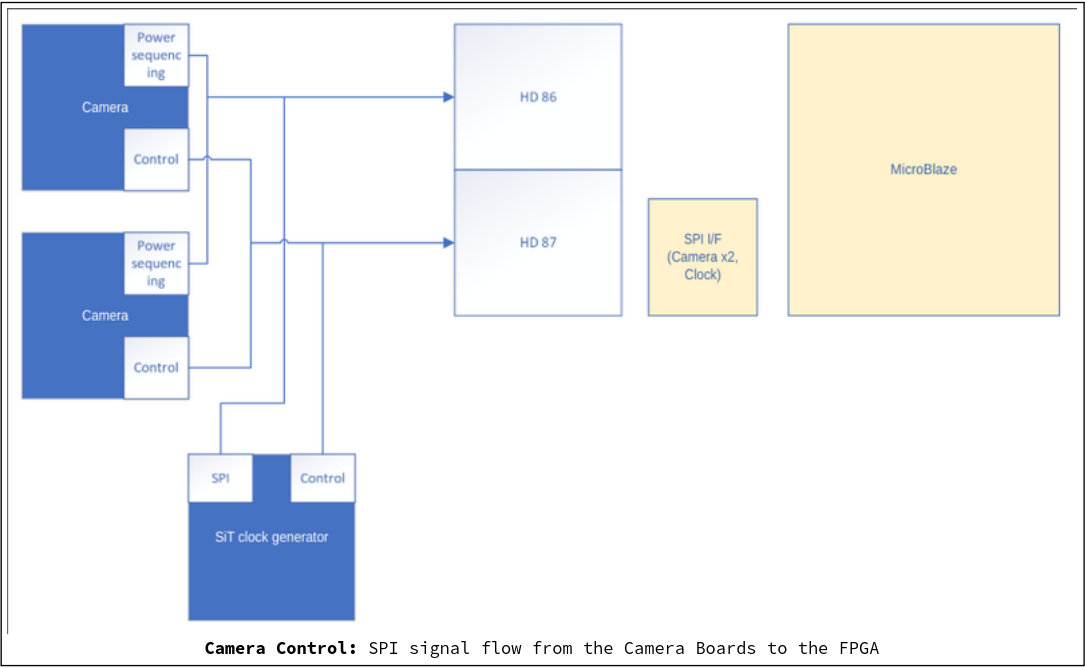
The microprocessors on the Camera Boards are for power sequencing only (hence the label "Power Sequencing"). The Image Sensors on the Camera Boards have a variety of control signals though, including:
- Triggers: E.g. signals that start and stop the process of capturing an image.
- HSYNC: Indicates that one line of the frame is transmitted.
- VSYNC: Indicates that an entire frame is transferred.
- SPI configuration: E.g. clock frequency, data bit lengths, etc.
Other camera settings also include aperture length and exposure time. This is explained in more detail in the next section.
1.2 FPGA -> Host
The final diagram indicates the PCI Express signal flow from the FPGA to the Host (Simula's onboard computer):
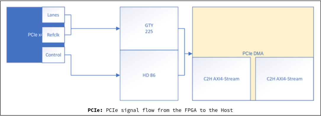
Note that the large blue box on the left labeled "PCIe" denotes the Host. "C2H" stands for "card-to-host". "PCIe DMA" (labeled orange) stands for "Direct Memory Access", and is what allow the Host to directly grab the processed FPGA data (used for Simula's AR Mode).
2 Image Processing Pipeline
After image data arrives to the FPGA from the Camera Boards, it is subjected to a multi-stage image processing pipeline before being handed off to the Host:
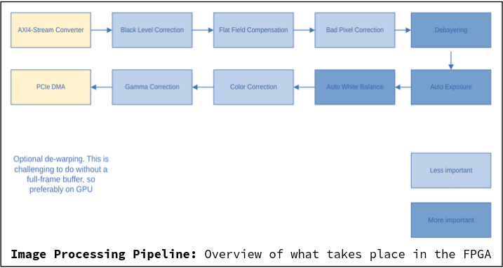
Below we review each of these steps.
2.1 Black Level & Flat Field Correction
A pixel's "black point" refers to the minimum brightness value that it can have, given a sensor/configuration. In theory, every pixel's "black point" should be 0; in practice, this isn't always true. Black level correction is then a process that force-adjusts the black point of each pixel to 0.
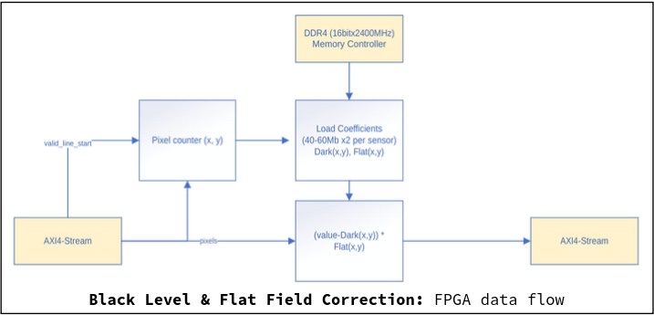
Similarly, flat field correction cancels the effects of image artifacts caused by variations in the pixel-to-pixel sensitivity of an image sensor and/or the non-uniformity of the camera lenses.
To do this, a "flat-field image" is captured from a uniform, featureless surface (such as a screen or lens cap). The uniform image is then used a reference to detect for unwanted variations in the brightness across the pixels, which can then later be corrected for via adjustments:
In our FPGA, both processes can be visualized as follows:
- Here, the load coefficients refer to the brightness values of each image sensor pixel.
Dark(x,y)refers to a pixel's brightness when the sensor covered/made dark.Flat(x,y)refers to the adjustment factor determined from the "flat field" test
2.2 Bad Pixel Correction
Image sensors can have defective pixels that fail to sense light levels correctly. In our FPGA pipeline, we check for defective pixels and then replace them with the average value of surrounding pixels:
![]()
2.3 Debayering
Debayering (also referred to as "demosaicing") refers to the process of converting a mosaic patterned image of R,G, or B pixels into a full-color image.
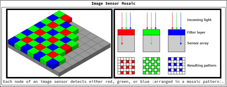
Under the hood, an image sensor (like our Sony IMX547) contains a grid of non-overlapping Red, Green, and Blue photosensors. As light hits the sensor, each of these photosensors only detects its corresponding color (red, green, or blue). This means the image sensor lacks complete color data in every node, which necessitates further image processing (in our FPGA) to interpolate the missing color details.
As an example, the following (non-overlapping) photosensor nodes are split up into red, green, and blue photosensor nodes:
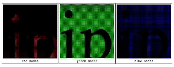
As can be seen above, an (e.g.) "red" node in the sensor lacks "green" and "blue" data. To fill in for the missing color data, a process called "demosaicing" has to be undertaken, which interpolates the unknown color data for each node:
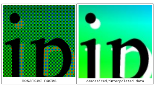
The end result is a recognizable image with full color data in every pixel.
2.4 Auto Exposure
Auto Exposure refers to the automatic adjusting of exposure time and aperture length to produce a well-exposed image.
- Exposure time: Length of time that the image sensor is exposed to light
- Aperture length: Size of opening of the camera's lenses
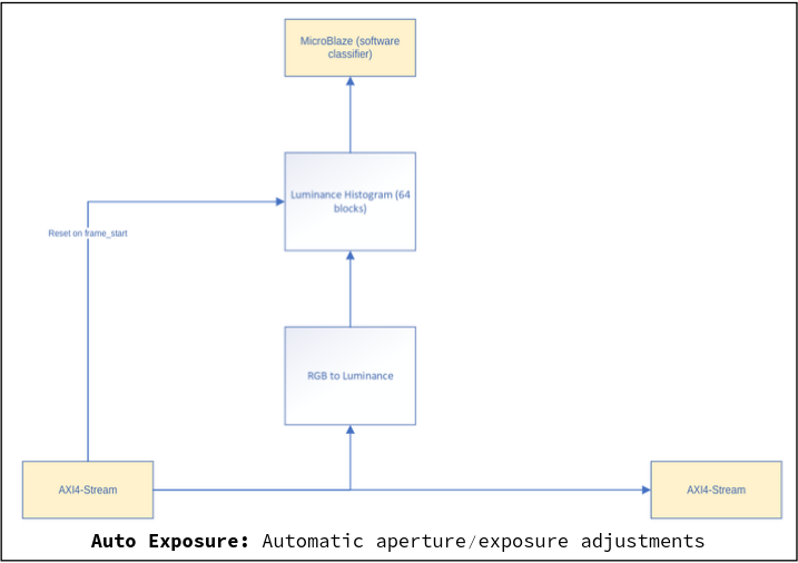
In the FPGA, we take a full frame of pixels, convert them into a luminance histogram, and then feed the data into our soft microcontroller ("MicroBlaze"). This then sends signals back to the Camera Boards to adjust the aperture/exposure settings accordingly.
2.5 Auto White Balance
Auto White Balance refers to the process of automatically adjusting the colors in an image to neutralize the color cast caused by different lighting conditions. Algorithmically, we use the "Gray World Assumption" for this, or the assumption that the average color of any image ought to be a neutral gray:
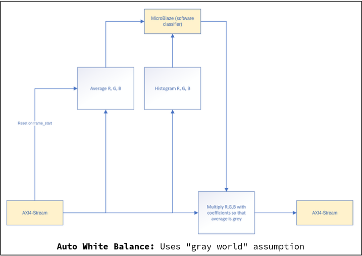
Each frame, we take grab the pixels and multiply/adjust them so that so that the transformed frame's average value is a neutral gray.
2.6 Color Correction
While white balance aims to remove color casts in an image by making the colors appear more neutral, color correction aims to improve the overall color representation and saturation of an image:
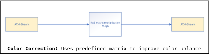
In the FPGA, the colors are adjusted on image frames based on a pre-defined matrix to produce a desired color balance.
2.7 Gamma Correction
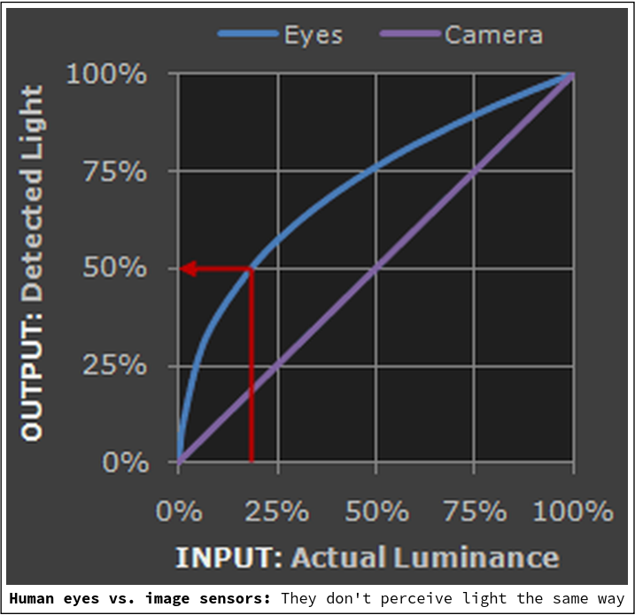
Gamma correction adjusts the shades captured by digital cameras to better match how they should appear to our actual eyes. Consider:
- Image sensors (linear). When twice the number of photos hit an image sensor, it receives twice the signal.
- Human eyes (non-linear). When twice the number of photos hit our eyes, our eyes perceive it as only a fraction brighter (nonlinearly).
The purpose of gamma correction is to correct for this discrepency. Pixel tones are redistributed so that they are closer to how our human eyes perceive them.
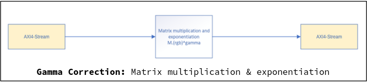
In the FPGA, gamma correction is undertaken by simple matrix multiplication and exponentiation. Note that Gamma correction can also be done on the GPU during rendering instead of the FPGA. (In fact, pretty much anything that just modifies the debayered image can be done on the GPU instead).